CAM350
Overview
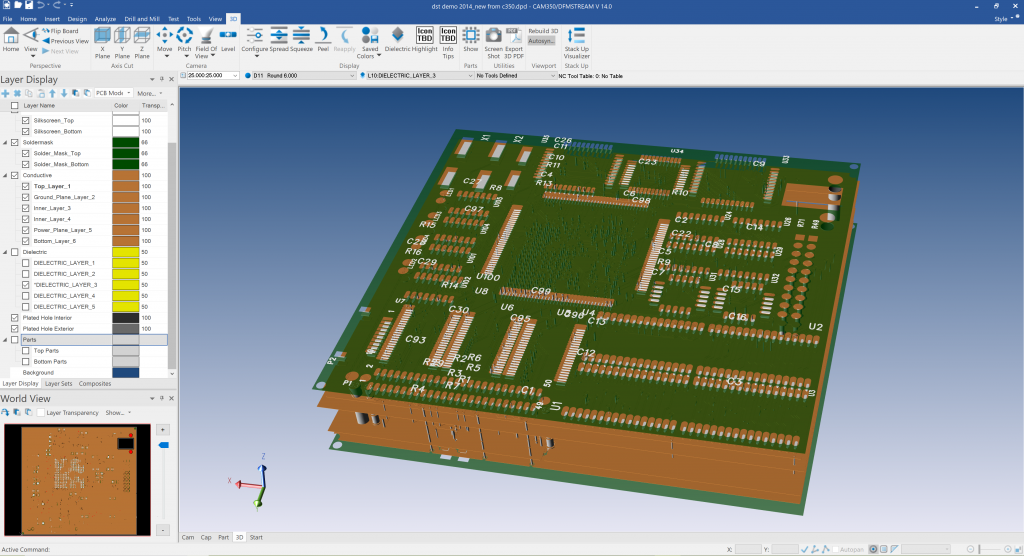
CAM350 offers a complete PCB Fabrication Flow that Streamlines the transition of engineering data into a physical PCB. This powerful solution provides superior price/performance in an easy-to-use product suite and delivers fast and accurate results.
CAM350 streamlines the electronic product delivery process by verifying and optimizing a PCB design for fabrication. CAM350 is easy to learn and use, and its return on investment is instantaneous. CAM350 gets PCB designs successfully through fabrication with ease – the first time.
Many electronic design organizations now recognize that problems arising during PCB fabrication can drastically impact product schedules, cause costly design re-spins, and require modifications to the design after release from engineering, compromising design integrity and intent. Inspecting, preparing and validating the PCB design prior to release to manufacturing will result in a significant increase in efficiency, less risk of design re-spin, and, most importantly, successful electronic products, built faster, at less cost.
Inspect, Prepare, and Validate
CAM350 will automatically import your CAD database or you can choose to import Gerber files. It will then use Netlist Compare to verify that the electrical characteristics of the Gerber layers match the design intent. Errors can occur in translation, operator mistakes, accidental inclusion of non electrical items in Gerber output, and problems with manual separation of voltages on a plane layer (2d lines on CAM plane in PowerPCB for instance). Netlist Compare will graphically match up original design files with Gerbers to ensure accuracy by locating any disparities.

CAM350 also offers Design Rule Checks (DRC) to verify the Gerber layers match not only the design rules in your CAD system, but the capabilities of your fabricator as well. CAM350’s Design for Fabrication (DFF) tools insure the board not only matches manufacturing capabilities, but also searches out design flaws that may affect yields resulting in missed deliveries and delayed product release. DFF can also detect failures that may escape traditional electrical verification.
CAM350’s Design for Fabrication (DFF) Analysis pulls fabrication rules into the PCB design domain and presents them in a way that is understood by the PCB designer. DFF Analysis verifies the PCB database, while still in engineering, seeking issues that may cause problems when entering into the fabrication process.
Key Features
- Analyze, identify, and fix manufacturing flaws that may cause delay
- Inspect for etching, soldermask, thermal, and spacing violations
- Verify and maintain design integrity and intent
Key Benefits
- State-of-the-art bare board testing
- Improved quality control
- Fewer shorts and design re-spins
- Directly import your design data for true WYSIWYG representations
Interested in CAM350?
Contact us to Learn More
Tools for PCB

HyperLynx
Unified Design & Verification
HyperLynx is industry-renowned for ease of use, with automated workflows that make sophisticated PCB analysis accessible to designers new to power and signal integrity analysis.

BluePrint-PCB
PCB Documentation
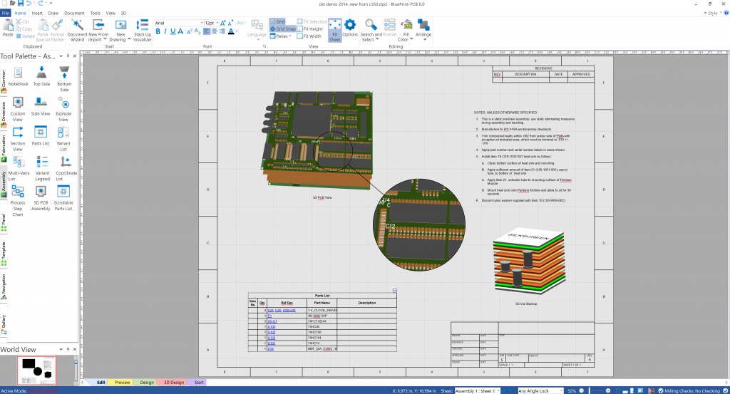
BluePrint is a revolutionary new document authoring tool that automates the PCB documentation process. It is also a state-of-the-art process for sharing and viewing documentation. BluePrint-PCB …

CAM350
Verify & Optimise
CAM350 offers a complete PCB Fabrication Flow that Streamlines the transition of engineering data into a physical PCB. This powerful solution provides superior price/performance in an easy …

